June 16, 2021
Novel Crystal Technology, Inc.
High-quality 100-mm β-type gallium-oxide epitaxial wafers were developed.
-β-type gallium oxide power devices can be mass produced.-
We successfully scaled up our high-quality gallium oxide epitaxial wafer manufacturing technology to 100-mm; gallium oxide power devices can now be produced on a 100-mm mass-production line.
With help from the New Energy and Industrial Technology Development Organization (NEDO), Novel Crystal Technology, Inc. (Sayama, Saitama, Japan, President & CEO Akito Kuramata) has developed high-quality 100-mm β-type gallium oxide (β-Ga2O3) epitaxial wafers1. With this success, low-loss β-Ga2O3 power devices can now be mass produced.
Typical semiconductor power devices such as Schottky barrier diodes (SBD)2 and transistors3 (hereinafter referred to as power devices) are used in home electronics, automobiles, trains, industrial machines, and in various electrical devices. They are parts that control voltage and current. In particular, when a control voltage or current is applied to power devices, electrical energy is lost due to energy conversion. By reducing this energy conversion loss, the power consumption of electrical equipment can be reduced. This can be considered a measure against global warming as it will lead to a reduction in CO2 emissions.
Compared with materials currently in development for use in power devices, such as silicon carbide (SiC) and gallium nitride (GaN), β-Ga2O3 has a larger band-gap energy4 of 4.5 eV5, and it is considered to be an ideal material because it can reduce the loss in power devices. Moreover, β-Ga2O3 is different from SiC and GaN in that single-crystal substrates can be fabricated with the melt growth method6. High-quality, large single crystals can be grown at 100 times the rate of SiC and GaN, leading to reduced costs. Thanks to these characteristics, the focus is on achieving practical use of β-Ga2O3 power devices in a timely manner. Corporations and research institutions around the world are accelerating their research and development.
■Contents
We succeeded in fabricating high-quality 2-inch (50.8 mm) gallium oxide epitaxial wafers in 2019 (see our press release dated April 18, 2019) and have been manufacturing and selling them since the beginning of 2019. However, there is as yet no 2-inch mass-production line for power devices because the manufacturing cost of the devices on 2 inch wafers is too high, and consequently, the use of these wafers has been limited to research and development. Recently, we developed 100-mm β-Ga2O3 epitaxial deposition equipment by applying our high-quality 2-inch epitaxial wafer technology. This advance means that high-quality100-mm β-Ga2O3 epitaxial wafers can now be produced and sold. In particular, β-Ga2O3 power devices can be produced on a 100-mm mass-production line.
In 2015, Novel Crystal Technology, Inc. collaborated with Professor Yoshinao Kumagai and Associate Professor Hisashi Murakami of Tokyo University of Agriculture and Technology and the National Institute of Information and Communications Technology in the development of a gallium-oxide halide vapor phase epitaxy7 for β-Ga2O3 epitaxial deposition. We have continued to improve the deposition equipment and process so that this technology can be applied to large wafers. Figure 1 shows a photograph of prototype β-Ga2O3 SBDs fabricated on 100-mm β-Ga2O3 epitaxial wafers. The epitaxial film is about 10-μm thick, and the donor concentration is about 2×1016 cm-3.
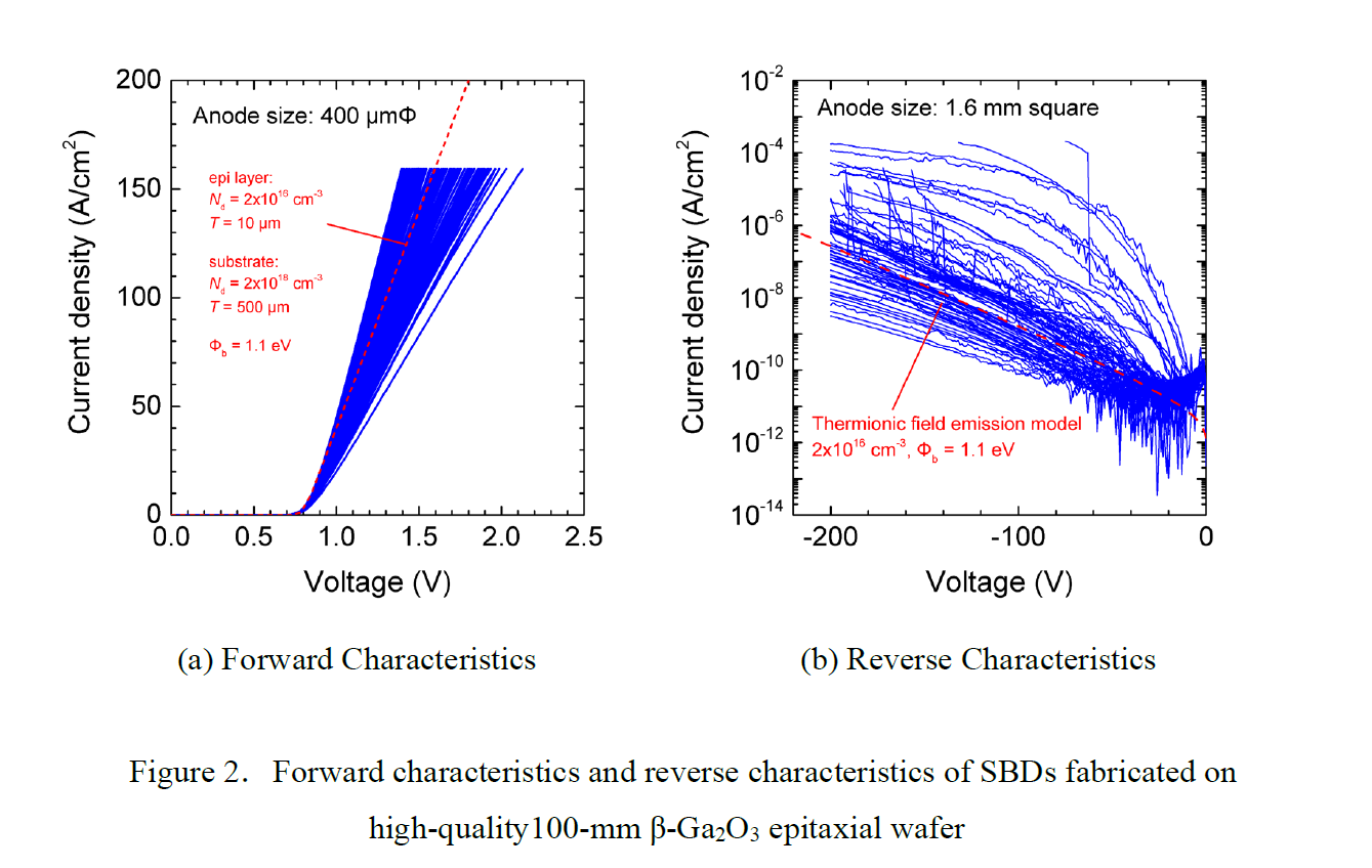
The yellow circles and squares on the wafer surface are gallium-oxide SBDs with different element sizes. Figure 2 shows the current-voltage characteristics of the diode. The measurements of 86 elements on the wafer surface are overlaid on each graph. The theoretical characteristics are drawn with a red dotted line in the graph. The forward characteristics in Fig. 2 (a) show that the current increases linearly from a low rising voltage of 0.8-0.9 V, and ideal diode characteristics are obtained.
The graph of the reverse characteristics in Fig. 2 (b) shows that 62 of the 86 elements show characteristics in line with the theoretical ones, and they can be judged as non-defective products. The killer defect density8 calculated from this non-defective rate is 13 pieces/cm2. This means that the 100-mm epitaxial wafer has the same quality as a high-quality 2-inch epitaxial wafer. Accordingly, 10-A β-Ga2O3 power devices can be produced on a 100-mm wafer with a yield of 80%.
■Future developments
We have started selling high-quality100-mm β-Ga2O3 epitaxial wafers as of today. Customers can specify the donor concentration of the epitaxial wafer in a range between 2×1016 cm-3 and 9×1016 cm-3.
Moreover, the epitaxial film thickness can be specified to between 5 μm and 10 μm. In the future, we will work to expand the specifiable ranges of donor concentration and film thickness, further reduce killer defects, and increase the wafer diameter.
We have already succeeded in demonstrating low-loss β-Ga2O3 SBDs with a trench structure9 (see our press release dated September 12, 2017). In the future, we will continue to build mass-production technology for trench-type SBDs on a 100-mm line. 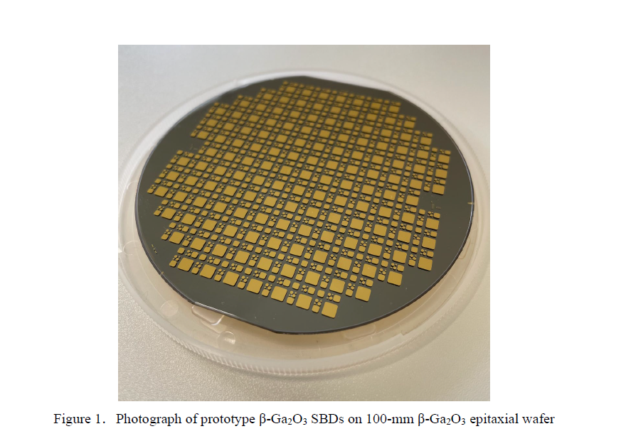
■Glossary
1 Epitaxial wafer
A wafer in which a crystal film is formed on a single crystal substrate. The quality of the crystal film is important mainly because the crystal film has a function.
2 Schottky barrier diode (SBD)
A diode that utilizes the electric potential barrier that occurs when a Schottky diode and a semiconductor are joined. It is characterized by a low forward voltage and low switching loss.
3 Transistor
A semiconductor device capable of amplification and switch operations. There are various kinds of transistor, such as MOSFET, thyristor, and IGBT, with various constructions and operating principles.
4 Bandgap energy
An energy state where electrons cannot exist between the lowest energy level of the conduction band and the highest energy level of the valence band in a solid. Semiconductors exist within this gap, and depending on the size of the bandgap, the conduction characteristics will change greatly.
5 eV (electron volt)
1 eV represents the energy of a single electron when accelerated at 1 V as it moves freely in space.
6 Melt growth method
A method by which materials to be crystallized are heated in a crucible past their melting point, and when melted, are brought into contact with the seed crystal and slowly reduced in temperature to produce a single crystal. The Czochralski, floating zone, and edge-defined film-fed growth method are famous examples.
7 Halide vapor phase epitaxy
One method of generating chemical vapors. The name originates from the use of halide in the source gas. To make a gallium oxide film, gallium chloride is usually used as the source gas.
8 Killer defect density
A killer defect is any one of a number of defects that cause serious deterioration in the characteristics of devices. Defects due to crystal imperfections, polishing scratches on the wafer surface, device process defects, etc. can be killer defects. In order to manufacture a large (large current) device with a high yield, it is important to reduce the density of killer defects.
9 Trench structure
A trench-like structure formed on the surface of the semiconductor by using etching technology.
■Contact
Novel Crystal Technology, Inc.
《Research information》Sales Department TEL:+81-3-6222-9336
《Press information》As above
Novel Crystal Technology is a carve-out venture of Tamura Corporation, who performs the development, manufacture, and sales of β-Ga2O3 substrates and epitaxial wafers. It is a technology transfer venture of the National Institute of Information and Communications Technology (NICT).