Taiyo Nippon Sanso Co., Ltd.
Tokyo University of Agriculture and Technology
New Energy and Industrial Technology Development Organization
March 1, 2022
World’s first successful epitaxial deposition of gallium oxide on a 6-inch wafer using the HVPE method
-Helping to reduce the cost of power devices and increase the energy savings of next-generation EVs-
As part of NEDO’s “Strategic Energy Conservation Technology Innovation Program”, Novel Crystal Technology, Inc., in collaboration with Taiyo Nippon Sanso Co., Ltd. and Tokyo University of Agriculture and Technology, has succeeded for the first time in depositing β-Ga2O3, a next-generation semiconductor material, on a 6-inch wafer by using the halide vapor phase epitaxy (HVPE) method.
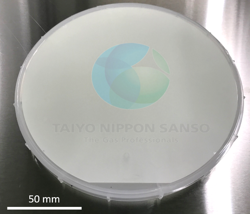 Fig. 1 β-Ga2O3 thin film formed on a 6-inch test wafer
Widespread adoption of β-Ga2O3 power devices is expected to lead to energy savings for inverters used in industrial machinery, residential photovoltaic power generation systems, and next-generation EVs. Our recent achievement will overcome the issue of the high cost of epitaxial deposition of β-Ga2O3 and lead to epitaxial deposition equipment capable of mass-producing large-diameter and epitaxial wafers.
1. Overview
Gallium oxide (β-Ga2O3)1) has a larger bandgap energy2) than silicon carbide (SiC)3) or gallium nitride (GaN) 4), and transistors and diodes made from this material are expected to have excellent power-device 5) characteristics, such as high breakdown voltage, high output, and high efficiency (low loss). Japan leads the world in the development of β-Ga2O3 power devices, and Novel Crystal Technology, Inc. has already developed small-diameter 4-inch β-Ga2O3 epitaxial wafers6) using the halide vapor phase epitaxy (HVPE) method in 2021.7) We currently manufacture and sell these wafers.8)
Unlike SiC and GaN wafers, β-Ga2O3 wafers are advantageous for lowering the price of power devices because they can be manufactured in the melt growth method in which bulk crystals grow quickly and it is easy to obtain a large-diameter wafer. However, while the HVPE method has a low raw-material cost and provides a high-purity deposition, the current equipment can make only small diameter (2 inches or 4 inches) single wafers. This problem means there is great demand for equipment capable of mass-producing large-diameter (6 inch or 8 inch) wafers in batches in order to reduce the epitaxial deposition cost involved in the HVPE method.
We have been working with Taiyo Nippon Sanso and Tokyo University of Agriculture and Technology to develop epitaxial deposition equipment for mass-producing large-diameter β-Ga2O3 wafers in NEDO’s “Strategic Energy Conservation Technology Innovation Program9) / Large-diameter mass-produced gallium oxide for next-generation power devices” project. In particular, we developed external supply technology10) for the metal chloride11) that is the raw material of the HVPE method during the “incubation” research and development phase of this program in FY2019. Moreover, we set up 6-inch single-wafer HVPE equipment and evaluated it to establish the basic technology of mass production in the practical development phase in FY2020-2021. This year, we succeeded in depositing β-Ga2O3 on a 6-inch wafer for the first time in the world.
2. Current achievements
Taiyo Nippon Sanso, Tokyo University of Agriculture and Technology and Novel Crystal Technology have developed a 6-inch single-wafer HVPE equipment (Fig. 2) and succeeded in depositing β-Ga2O3 on a 6-inch test wafer (using a sapphire substrate) for the first time in the world (Figure 1).
In addition, we demonstrated β-Ga2O3 epitaxial deposition on a 6-inch test wafer and achieved a film thickness distribution of ± 10% or less and furthermore confirmed that uniform epitaxial deposition is possible (Fig. 3) by optimizing the epitaxial deposition conditions and using a unique raw-material nozzle structure. These achievements will greatly advance the development of the large-diameter-wafer batch-type mass-production equipment. It is estimated that the energy saving effect of the β-Ga2O3 epitaxial deposition process and mass adoption of devices will be about 210,000 kL/year by 2030.
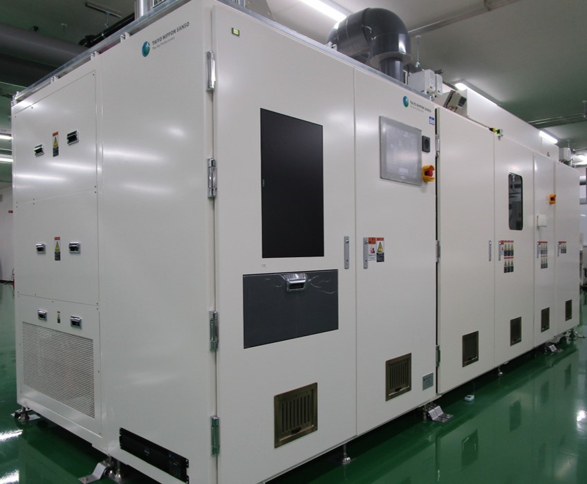 Fig. 2 Photograph of the developed 6-inch single-wafer HVPE equipment
for β-Ga2O3 epitaxial deposition
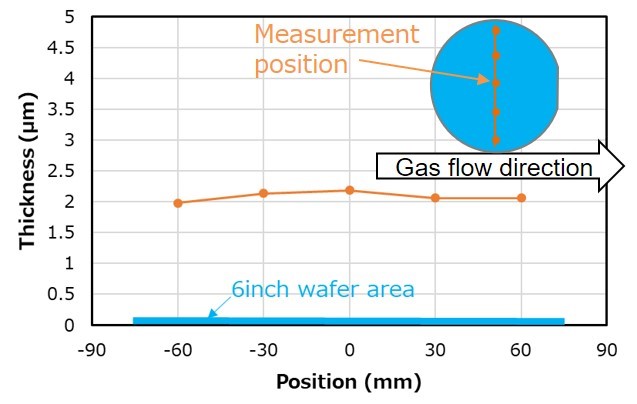
Fig. 3 Film thickness distribution of β-Ga2O3 on a 6-inch test wafer
3. Future plans
Taiyo Nippon Sanso, Tokyo University of Agriculture and Technology and Novel Crystal Technology will continue to develop mass-production equipment for β-Ga2O3 epitaxial deposition in the NEDO project and perform epitaxial film deposition using 6-inch β-Ga2O3 wafers and β-Ga2O3 thin film. We will develop high-quality β-Ga2O3 epitaxial deposition technology by evaluating the electrical characteristics and defects existing in the film and aim to commercialize the equipment in 2024. β-Ga2O3 epitaxial wafers manufactured by the HVPE method are mainly used for SBDs12) and FETs13), and the market is expected to grow to about 59 billion yen by 2030.14) By entering the market with our mass-production equipment and popularizing β-Ga2O3 power devices, we will provide energy savings for next-generation EVs and other power applications.
[Notes]
1 Gallium oxide (β-Ga2O3) 2 Gallium nitride (GaN) 3 Silicon carbide (SiC) 4 Bandgap energy 5 Power device 6 β-Ga2O3 epitaxial wafer 7 Halide vapor phase epitaxy (HVPE) method 8 4-inch β-Ga2O3 epitaxial wafers now available; opportunities for manufacturing and sales 9 Strategic energy-saving technology innovation program 10 External supply technology 11 Metal chloride 12 SBD 13 FET 14 Quoted from Fuji Keizai
Gallium oxide is a compound semiconductor that is attracting attention as a third wide bandgap semiconductor for power devices following the adoption of silicon carbide and gallium nitride. Its theoretical performance as a power device is overwhelmingly higher than that of silicon and surpasses that of silicon carbide and gallium nitride.
GaN is a compound of gallium and nitrogen and is a wide-bandgap semiconductor with a more stable bond structure and higher dielectric breakdown strength than SiC. It is mainly used for small and high-frequency applications such as switching power supplies.
SiC is a compound of carbon and silicon and is a wide-bandgap semiconductor material mainly used for high-breakdown-voltage and high-current applications.
The energy required for electrons and holes to transition from the valence band to the conduction band. A semiconductor with a large value is called a wide-bandgap semiconductor, and the larger the bandgap, the higher the dielectric breakdown strength. The bandgap of β-Ga2O3 is about 4.5 eV, which is larger than that of Si (1.1 eV), 4H-SiC (3.3 eV) or GaN (3.4 eV).
A semiconductor element used for power conversion in power inverters and converters.
A wafer with a thin film of β-Ga2O3 deposited on the wafer substrate. Crystal growth is performed on seed crystals that will become the wafer. Growth in which the atoms of the thin film are aligned to the crystal plane of the underlying wafer is called epitaxial growth.
A crystal growth method that utilizes metal chloride gas as a raw material. Its advantages are that high-speed growth and high-purity epitaxial deposition are possible with it.
Novel Crystal Technology, Inc. News release dated June 16, 2021
High-quality 100-mm β-type gallium oxide epitaxial wafers have been developed.
Summary at https://www.nedo.go.jp/english/activities/activities_ZZJP_100039.html
In the HVPE method, this technology separates the metal chloride generation part and the epitaxial deposition part and supplies metal chloride from the outside of the reactor through piping.
A compound that is a raw material in the HVPE method: typical metal chlorides include GaCl, GaCl3, AlCl, AlCl3, InCl, and InCl3.
Schottky Barrier Diode. A diode that utilizes a junction made of a certain metal and an n-type semiconductor instead of a PN junction. Its advantages are higher efficiency and faster switching than other diodes.
Field Effect Transistor (FET). A transistor that controls the current between source and drain electrodes by applying a voltage to a gate electrode to vary the density of electrons or holes in the channel region.
Quoted from Fuji Keizai “2020 Current Status and Future Prospects of the Next Generation Power Devices & Power Electronics Related Equipment Market”
(Contact for inquiries regarding the contents of this news release)
Novel Crystal Technology:
Contact Person: Sasaki, TEL: +81-4-2900-0072
Taiyo Nippon Sanso:
Contact Person: Naito, TEL: +81-80-3755-3185
Tokyo University of Agriculture and Technology:
Contact Person: Kumagai, TEL: +81-42-388-7469
NEDO Energy Conservation Department:
Contact Person: Kitai, TEL: +81-44-520-5281