
World’s first inverted gallium oxide DI-MOS transistor
-Major progress in the development of gallium oxide power transistors –
Novel Crystal Technology, Inc. (Headquarters: Sayama City, Saitama Prefecture, President: Akito Kuramata) has confirmed the basic operation of a high-breakdown voltage (1 kV) gallium oxide inverted double implanted MOS transistor (DI-MOSFET) with a sufficiently high threshold voltage (6 V) as part of its involvement in the “Research and Development of Inverted MOS Channel Type Gallium Oxide Transistor” program of the National Security Technology Research Promotion Fund (JP004596) of the Acquisition, Technology & Logistics Agency..
This achievement, a world’s first for gallium oxide (β-Ga2O3), is groundbreaking and will greatly advance the development of medium-to-high voltage (0.6-10 kV) gallium-oxide transistors, which will in turn lead to lower prices and higher performance in power electronics. Moreover, it will contribute to the efficient use of electric energy in vehicles such as electric vehicles and flying cars by improving the efficiency and downsizing of power electronics equipment such as power converters for solar power generation, general-purpose inverters for industrial use, and power supplies. The details on this development were announced at the 83rd Japan Society of Applied Physics Autumn Meeting Symposium on September 21, 2022.
1. Overview
Compared with silicon carbide (SiC)1) and gallium nitride (GaN)2), which are also being developed as high-performance materials to replace silicon, gallium oxide (β-Ga2O3)3) has superior material properties and low-loss, low-cost power devices4) can be made with it by using a low-cost crystal growth method. β-Ga2O3 is expected to be useful in various power electronics equipment, such as home appliances, electric vehicles, railway vehicles, industrial equipment, solar power generators, and wind power generators. In addition, domestic and foreign companies and research institutes are accelerating their research and development on β-Ga2O3 because they see the material as a way to reduce the size and improve the efficiency of installed electrical equipment.
Novel Crystal Technology, Inc. has been aiming to commercialize the β-Ga2O3 transistor since 2019
by participating in the “Research and Development of Inverted MOS Channel Type Gallium Oxide Transistor” program of the National Security Technology Research Promotion Fund (JP004596) of the Acquisition, Technology & Logistics Agency. It is now the first organization in the world to succeed in operating a gallium oxide inverted double-implanted MOS transistor (DI-MOSFET)5) with a high breakdown voltage (1 kV) and sufficiently high threshold voltage6) (6.6 V). The high-resistivity Ga2O3 layer of the transistor is doped with nitrogen (N), an acceptor impurity7), through ion implantation8) and the well layer9) is given an activation heat treatmen10)
The company foresees rapid development of medium-to-high voltage (0.6-10 kV) gallium oxide transistors that will lead to lower priced and higher performance power electronics.
2. Results
Until now, normally-off β-Ga2O3 transistors have used a fin structure11) that does not require a p-type layer because the p-type conductive layer12) technology has not yet been established. However, the fin must have a fine structure of 0.4 μm or less with good dimensional control. It has been difficult to fabricate large devices such as this with a chip size of several millimeters square with good yield.
In response to this problem, Novel Crystal Technology, Inc. has been developing an inverted MOS channel structure that can be manufactured with high yield even using conventional stepper exposure equipment13) and dry etching equipment14). Instead of relying on developing the technically challenging β-Ga2O3 p-type conductive layer, the current development uses a high-resistance β-Ga2O3 layer doped with nitrogen (N) as an acceptor impurity and a well layer made through an activation heat treatment. In a mobility evaluation, the fabricated long-channel (LCH=100 μm) lateral transistor exhibited a high threshold voltage of 6.2 V, which could not be achieved with a fin structure, and a higher MOS channel mobility (52 cm2/Vs) than that of a device made from SiC (Fig. 1).
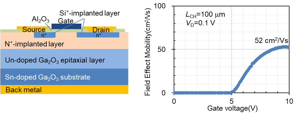
(a) Cross section (b) Field effect mobility of MOS channel
(Fig. 1) Cross section and channel mobility of long channel lateral transistor
Furthermore, an inverted DI-MOS transistor (Fig. 2) fabricated using this process had a threshold voltage of 6.6 V at an N+ ion implantation concentration of 1×18 cm-3 and had the off-stage voltage
of 1.1kV at an N+ ion implantation concentration of 3×18 cm-3 or higher. (Fig. 3). We found that the N+ ion-implanted high-resistance β-Ga2O3 layer works as a threshold voltage control layer and a current blocking layer in the same way as a p-type conductive layer. We believe that the channel length15) of the prototype DI-MOSFET was as long as 10 μm, and the on-resistance was as high as 153 mΩcm2. The newly developed DI-MOSFET device and process will enable large devices to be fabricated on 4-6 inch wafer mass production lines, and we can expect significant progress in the development of low-loss β-Ga2O3 power transistors.
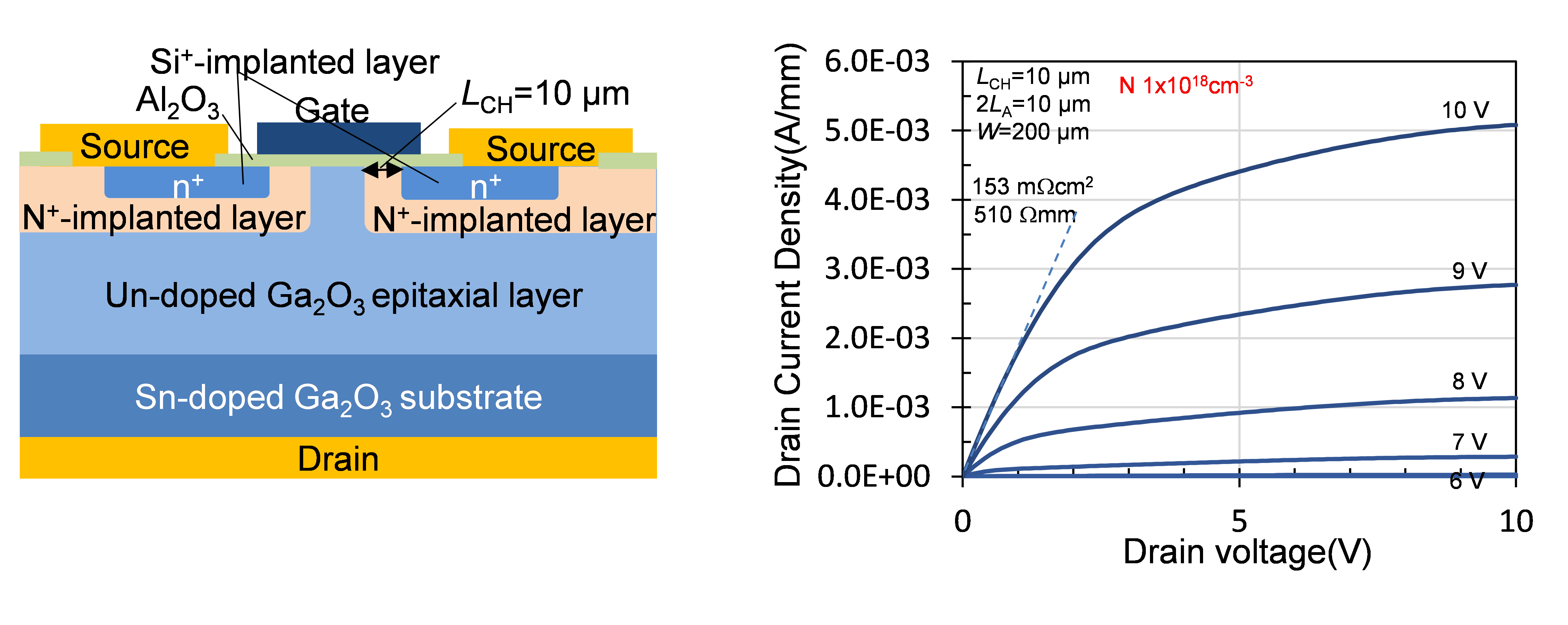
(a) Cross section (b) Static characteristics of transistor
(Fig. 2) Cross section and static characteristics of β-Ga2O3 DI-MOS transistor
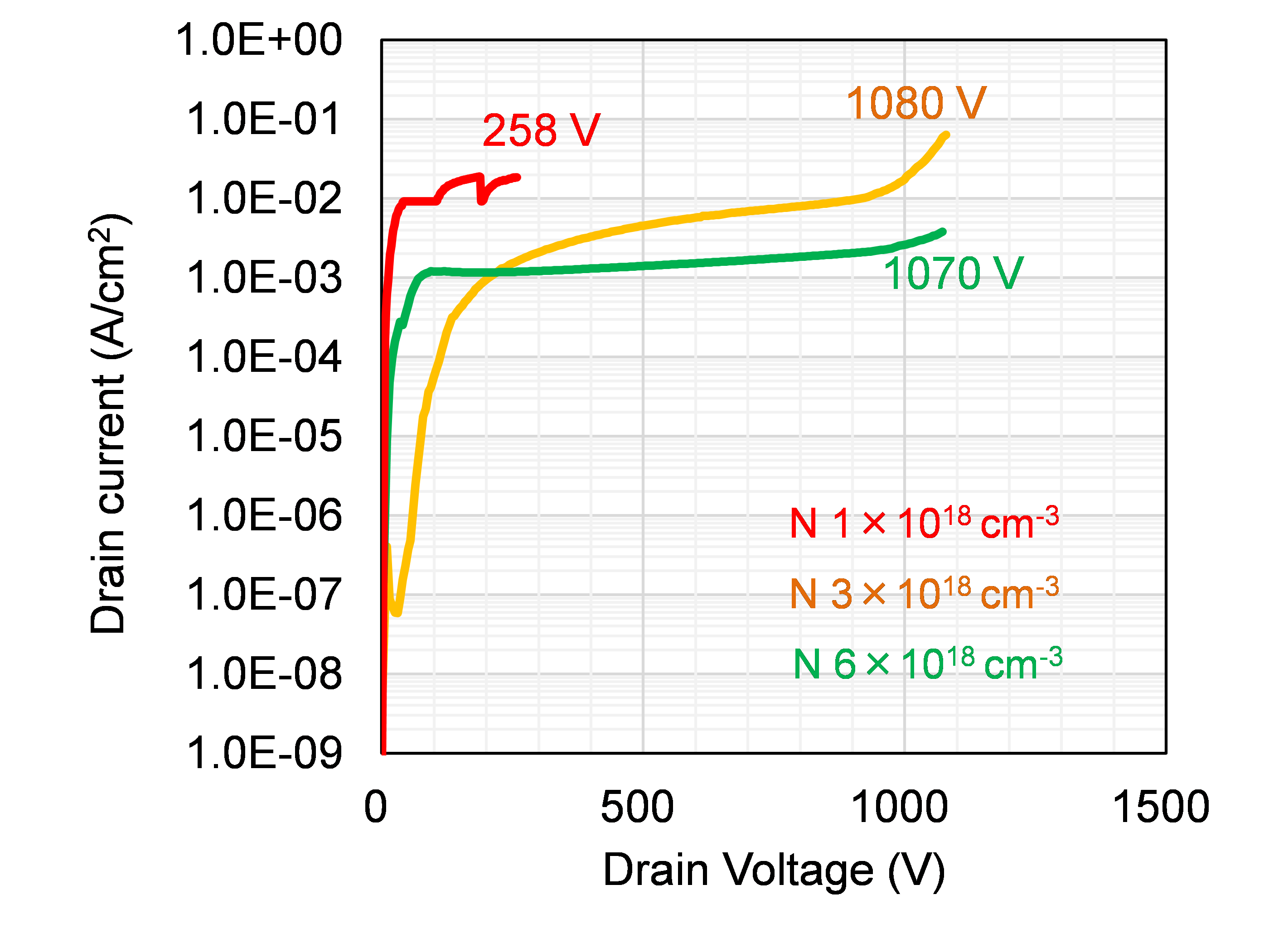
(Fig. 3) Breakdown voltage waveform of β-Ga2O3 DI-MOS transistor
3. Future plans
Novel Crystal Technology, Inc. will analyze the characteristics of the N-doped β-Ga2O3 high-resistance layer in the prototype inverted MOS transistor as part of the project commissioned by the Acquisition, Technology & Logistics Agency. In addition, it will conduct trial production on a 4-inch mass production foundry line, improve the device characteristics, and ensure reliability. It will also proceed with the development of a full β-Ga2O3 power module combined with a gallium oxide Schottky barrier diode (SBD)16) that is now being commercialized.
The market size for medium- and high-voltage high-speed transistors and high-speed diodes is expected to expand to 7.9 billion yen by 2025 and 47 billion yen by 2030.17) Novel Crystal Technology Co., Ltd. will enter this market with β-Ga2O3 transistors, SBDs, and full β-Ga2O3 modules with the goal of contributing to the energy-saving society.
【Notes】
1 Silicon carbide (SiC)
A compound of silicon and carbon, it is one of the wide-gap semiconductors.
2 Gallium nitride (GaN)
A compound of gallium and nitrogen, it is one of the wide-gap semiconductors.
3 Gallium oxide (β-Ga2O3)
A compound of gallium and oxygen, it is one of the wide-gap semiconductors.
4 Power device
A semiconductor element that can control a high voltage and high current and is used in power conversion equipment such as inverters.
5 Inverted double implanted MOS transistor (DI-MOSFET)
This is a MOS field effect transistor formed by ion-implanting two types of impurities, which form an n-type layer and a p-type (high resistance) layer, into the required regions in two separate steps. In the inversion type, when a positive voltage is applied to the gate, electrons accumulate at the insulating film/p-type (high resistance) layer interface, causing current to flow.
6 Threshold voltage
The voltage at the gate at which current begins to flow in a transistor.
7 Acceptor impurity
Impurities in semiconductors that capture electrons and become negatively charged. In general, by capturing electrons, holes are generated in the semiconductor, making it a p-type semiconductor.
8 Ion implantation
This is one of the technologies for adding impurities to semiconductors. Impurity atoms are ionized, accelerated with a voltage of several tens to several hundred kV, and implanted into the semiconductor.
9 Well layer
A layer in a transistor whose current is controlled by the gate.
10 Activation heat treatment
This is a heat treatment that restores the damage that the semiconductor received during ion implantation and promotes the electrical function of the implanted impurities. Temperatures of 600-1200°C are usually used.
11 Fin structure
A structure in which the gate is located on two sides of the channel or wraps around the channel to form a double gate. It is called a fin structure because it has the shape of a fin (fish fin).
12 p-type conductive layer
A semiconductor layer in which the particles that conduct current in a conductive semiconductor are holes rather than electrons.
13 Stepper exposure device
This is a reduction projection exposure system widely used in semiconductor mass production lines.
14 Dry etching equipment
This equipment performs fine processing of insulating films and semiconductor materials by discharging reactive gas in a vacuum.
15 Channel length
This is the length of the area in the current direction of the transistor where the current is controlled by the gate.
16 Schottky barrier diode (SBD)
This is a diode that utilizes the rectification property that current flows only in one direction when a semiconductor and a metal are joined together in what is called a Schottky junction. Schottky junction diodes have the advantage of lower switching losses than PN junction diodes.
17 Quoted from Fuji Keizai market report article “2022 Current Status and Future Prospects of the
Next Generation Power Devices & Power Electronics Related Equipment Market”
(Contact for inquiries regarding the contents of this news release)
Novel Crystal Technology, Sales Department:
Contact Person: Masui, TEL: +81-3-6222-9336
Novel Crystal Technology is a carve-out venture of Tamura Corporation, and is involved in the development, manufacture, and sales of β-Ga2O3 substrates and epitaxial wafers. It is a technology transfer venture of the National Institute of Information and Communications Technology (NICT).