April 18, 2019
Novel Crystal Technology, Inc.
Saga University
TAMURA Corporation
Development of high-quality β-type gallium oxide film growth technique has been achieved
-Next goal is gallium oxide power devices with high currents-
By reducing defects in the crystals of the gallium oxide film it is possible to significantly decrease leakage current in gallium oxide power devices. It is now possible to produce 10-A high-current devices.
With help from the New Energy and Industrial Technology Development Organization (NEDO), Novel Crystal Technology, Inc. (Sayama, Saitama, Japan, President & CEO Akito Kuramata), and in collaboration with Saga University and TAMURA Corporation, a high-quality, β-type gallium oxide (β-Ga2O3) epitaxial film※1 has been recently developed. With this success, ultra-low-loss high-current β-Ga2O3 power devices can be mass produced.
Typical semiconductor power devices such as Schottky barrier diodes (SBD)※2 and transistors※3 (hereinafter referred to as “power devices”) are used in home electronics, automobiles, trains, industrial machines, and in other electric devices around the world. They are a part that controls voltage and current. When the control is applied, electric current flows in the device, but the electrical resistance is high, leading to a loss of electrical energy. For example, in the case of electric automobiles, they move thanks to electrical energy stored in the battery, however as electrical energy is lost due to energy conversion in the power device, the distance that can be traveled on one charge decreases. Consequently, it is important for electrical devices that the resistance in power devices be decreased (reduced loss).
Compared to materials currently in development for use in power devices, such as silicon carbide (SiC) and gallium nitride (GaN), β-Ga2O3 has a large band-gap energy※5 of 4.5 eV※4, and it is an ideal material because it will further reduce the loss in power devices. Moreover, β-Ga2O3 is different from SiC and GaN in that single-crystal substrates can be fabricated with the melt growth method※6. High-quality, large single crystals can be grown at 100 times the rate of SiC and GaN, leading to reduced costs. Thanks to these characteristics the focus is on achieving practical use of β-Ga2O3 power devices in a timely manner. Corporations and research institutions around the world are accelerating its research and development.
■Details
Prominent research institutions have reported on operational tests of β-Ga2O3 power devices. However, there were issues with the quality of the crystals on the β-Ga2O3 epitaxial film. As the chip size increases, leakage current※7 significantly increases. Only small chips with about 1-A current flow could be produced. In order to expand the use of β-Ga2O3 power devices into home electronics, automobiles, industrial machines, etc., it must become possible to create large chip that can handle current flow 10-A or more.
This time technology was developed that utilizes halide vapor phase epitaxy※8 to generate a β-Ga2O3 film. An assessment method was also developed. We were able to reduce crystal defects in the β-Ga2O3 film to 1/100 of our existing products. With this, leakage current in β-Ga2O3 power devices was significantly reduced, and it is now possible to produce large chips.
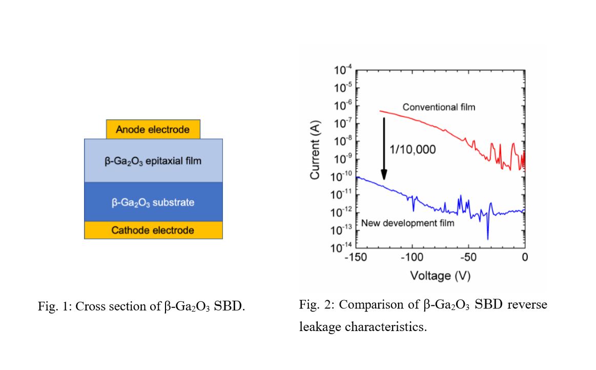
Figure 1 shows a cross section of the typical β-Ga2O3 SBD. Figure 2 shows a comparison of the reverse current-voltage (I-V) characteristics of a β-Ga2O3 SBD with an element size of φ500 μm produced with both conventional technology and the newly developed technology. The SBD produced in this trial had a leakage current that was 1/10,000 of the conventional product.
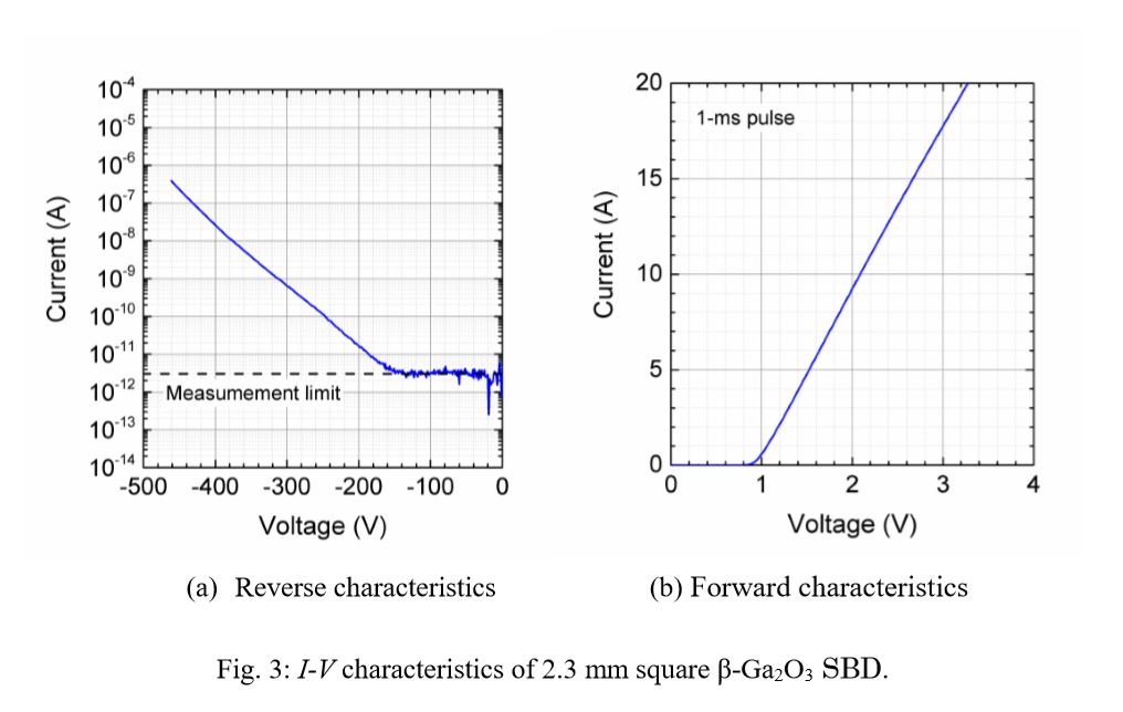
Figure 3 shows the I-V characteristics of 2.3-mm square β-Ga2O3 SBD that was created for the high-current operational test. While maintaining a sufficiently low reverse leakage current, operation was achieved at 20 A (20 times) the standard current.
We have already developed an SBD with a trench structure.※9 And we have successfully demonstrated a low-loss diode with a forward voltage※10 that is about 40 % lower than SiC (Refer to press release from September 12, 2017). The next goal is to apply the recently developed technology to trench-type SBDs. We will develop >10-A β-Ga2O3 SBDs with low forward loss. If this device can be realized, contributions towards energy saving in various electronic devices such as home electronics, automobiles, and industrial devices can be expected.
■Future developments
We intend to begin selling the newly developed β-Ga2O3 epitaxial wafers soon. From the second half of fiscal 2019, we will begin shipping samples of 10-30 A with breakdown voltage of, 650-V β-Ga2O3 trench-type SBDs. Our plan is to advance preparations for mass production starting in 2021. We are engaged in quickly developing a 100-A class β-Ga2O3 power device.
■Glossary
※1 Epitaxial film
Generates crystals on the crystal substrate. It is the crystal film arranged on the crystal surface of the substrate.
※2 Schottky barrier diode (SBD)
Diode that utilizes the electric potential barrier that occurs when a Schottky diode and a semiconductor are joined. It is characterized by a low forward voltage and low switching loss.
※3 Transistor
Semiconductor device that causes amplification or switch operations. There are various products such as MOSFET, Thyristor, IGBT, etc. with various constructions and operating principles.
※4 eV (electron volt)
1 eV represents the energy of a single electron when accelerated at 1 V as it moves freely in space.
※5 Bandgap energy
An energy state where electrons cannot exist between the lowest energy level of the conduction band and the highest energy level of the valence band in a solid. Semiconductors exist within this gap, and based on the size of the bandgap, the conduction characteristics will change greatly.
※6 Melt growth method
The method by which materials to be crystallized are heated in a crucible past their melting point, and when melted, are brought into contact with the seed crystal and slowly reduced in temperature to produce a single crystal. The Czochralski, floating zone, and edge-defined film-fed growth method are famous examples.
※7 Leakage current
Current that unintentionally flows in an off-state power device. Reducing leakage current is desirable.
※8 Halide vapor phase epitaxy
One method for generating chemical vapors. The name originates in the use of halide in the source gas. When generating a gallium oxide film, gallium chloride is usually used as the source gas.
※9 Trench structure
The trench-like structure formed on the surface of the semiconductor from the etching technology.
※10 Forward voltage
The reduction in voltage that occurs when a diode is on. Reducing forward voltage is desirable.
■Contact
Novel Crystal Technology, Inc.
《Research information》Sales department TEL:04-2900-0072
《Press information》As above
Saga University
《Research information》Department of Science and Engineering TEL:0952-28-8511
《Press information》General Affairs Department, General Affairs Section, Public Relations Office TEL:0952-28-8153
TAMURA Corporation
《Research information》Core Technology Head Office, Semicon Development Office
TEL:04-2900-0045
《Press information》 Business Management Head Office, Business Management Support Group
TEL:03-3978-2031
※Novel Crystal Technology is a carve-out venture of Tamura Corporation, who performs the development, manufacture, and sales of β-Ga2O3 substrates and epitaxial wafers. It is a technology transfer venture of the National Institute of Information and Communications Technology (NICT).