June 16, 2021
Novel Crystal Technology, Inc.
Gallium oxide vertical transistor with the world’s highest breakdown voltage
-4.2 kV is 1.6 times higher than the breakdown voltage of conventional transistors –
We have developed a gallium oxide vertical transistor with the world’s highest breakdown voltage
With help from the Security Technology Research Promotion System (JPJ004596) implemented by the Acquisition, Technology and Logistics Agency, Novel Crystal Technology, Inc. (Sayama, Saitama, Japan, President & CEO Akito Kuramata) has succeeded in developing a high-voltage gallium oxide (β-Ga2O3) vertical normal off MOS transistor1. We will use this result to accelerate the development of β-Ga2O3 power transistors.
Typical semiconductor power devices such as Schottky barrier diodes (SBD)2 and transistors3 (hereinafter referred to as power devices) are used in home electronics, automobiles, trains, industrial machines, and in various electrical devices. They are parts that control voltage and current. In particular, when a control voltage or current is applied to power devices, electrical energy is lost due to energy conversion. By reducing this energy conversion loss, the power consumption of electrical equipment can be reduced. This can be considered a measure against global warming as it will lead to a reduction in CO2 emissions.
Compared with materials currently in development for use in power devices, such as silicon carbide (SiC) and gallium nitride (GaN), β-Ga2O3 has a larger band-gap energy4 of 4.5 eV5, and it is considered to be an ideal material because it can reduce the loss in power devices. Moreover, β-Ga2O3 is different from SiC and GaN in that single-crystal substrates can be fabricated with the melt growth method6. High-quality, large single crystals can be grown at 100 times the rate of SiC and GaN, leading to reduced costs. Thanks to these characteristics, the focus is on achieving practical use of β-Ga2O3 power devices in a timely manner. Corporations and research institutions around the world are accelerating their research and development.
■Contents
We manufacture and sell β-Ga2O3 single-crystal substrates and epitaxial wafers7, and are developing SBDs and transistors with the aim of commercializing them.
Figure 1 shows a cross section of the newly developed β-Ga2O3 vertical MOS transistor.
The characteristics of the transistor are as follows:
・ A vertical device structure that is advantageous for meeting the low-loss and large-current requirements of power devices.
・ A FinFET8 structure that enables normally off operation without using a p-type conductive layer by narrowing the mesa width to submicron or less.
・ High dielectric constant hafnium oxide (HfO2) insulating film to weaken the electric field strength in the gate insulating film.
・ A high-voltage drift layer with a low donor concentration (4 x1015 cm-3) and thick film (40 μm) formed using our newly developed high-quality thick-film epitaxial growth technology.
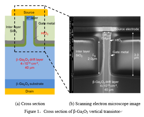
Figure 2 shows the drain current-drain voltage characteristics of the fabricated transistor (mesa width 0.4 μm, mesa length 60 μm). The device shows a normally off characteristic in which no current flows at a gate voltage of 0 V, a maximum current density of 2.6 mA/mm, and an on-resistance of 1.2 x 10³ Ω mm. In this transistor prototype, the source n+ layer and the channel layer are separated by about 0.4 μm, and it is estimated that the source resistance is high. We believe that it is possible to reduce the on-resistance further by improving the device design.
Figure 3 shows the gate voltage dependence of the drain current and gate current when a drain voltage of 5 V is applied. The drain current on/off ratio is as large as 8 digits or more, the subthreshold coefficient9 is 120 mV/decade, and the gate leakage current is below the measurement limit; good transistor characteristics are thus obtained. On the other hand, the drain current-gate voltage characteristic shows hysteresis of about 0.2 V, meaning that the MOS gate interface needs to be improved.
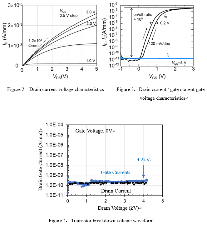
Figure 4 shows the drain current and gate current characteristics when a positive voltage is applied to the drain electrode with the gate voltage and source voltage fixed at 0 V. Due to the improved controllability of the gate afforded by the FinFET structure and the effect of the high dielectric constant HfO2 insulating film on the bottom surface of the mesa processing, no drain leak current or gate leak current is generated even if a drain voltage up to about 4 kV is applied. In addition, by adopting a high-quality epitaxial layer with a low donor concentration (4×1015 cm-3) and a thick film of 40 μm as the drift layer, a breakdown voltage of 4.2 kV (1.6 times the previously reported value of 2.6 kV (W. Li et al., IEDM 19-270)) is obtained. The maximum electric field strength in the β-Ga2O3 drift layer on the bottom surface of the mesa processing is estimated to be 2.5 MV/cm. A two-dimensional device simulation indicated that an electric field concentration several times stronger than this is generated at the gate electrode end. Therefore, the breakdown voltage can be further increased in the future by introducing an electrode termination structure that alleviates the electric field concentration. We believe that low on-resistance can be achieved.
■Future developments
In addition to solving the problems clarified by studying this device prototype, we will work to increase the size and current of the device. We will start mass production of 600-1200 V medium breakdown voltage devices in 2025 and prepare for mass production of high breakdown voltage devices of 3000 V or higher. The low cost of β-Ga2O3 semiconductors for use in the medium breakdown voltage region is an advantage for electric vehicles and other commercial applications. We will proceed with development to reach our goal.
■Glossary
1 MOS transistor
A transistor that controls drain current using a gate metal (metal) / insulating film (oxide) / semiconductor structure.
2 Schottky barrier diode (SBD)
A diode that utilizes the electric potential barrier that occurs when a Schottky diode and a semiconductor are joined. It is characterized by a low forward voltage and low switching loss.
3 Transistor
A semiconductor device capable of amplification and switch operations. There are various kinds of transistor, such as MOSFET, thyristor, and IGBT, with various constructions and operating principles.
4 eV (electron volt)
1 eV represents the energy of a single electron when accelerated at 1 V as it moves freely in space.
5 Bandgap energy
An energy state where electrons cannot exist between the lowest energy level of the conduction band and the highest energy level of the valence band in a solid. Semiconductors exist within this gap, and depending on the size of the bandgap, the conduction characteristics will vary greatly.
6 Melt growth method
A method by which materials to be crystallized are heated in a crucible past their melting point, and when melted, are brought into contact with a seed crystal and slowly reduced in temperature to produce a single crystal. The Czochralski, floating zone, and edge-defined film-fed growth method are famous examples.
7 Epitaxial wafer
A wafer in which a crystal film is formed on a single crystal substrate. The quality of the crystal film is important mainly because the crystal film has a function.
8 FinFET structure
A transistor in which the gate is located on two sides of the channel or surrounds the channel to form a double gate structure. It is called a FinFET because it has the shape of a fin (fish fin).
9 Subthreshold coefficient
A figure of merit that indicates the off performance of a transistor. The gate voltage required to increase the amount of current by an order of magnitude. The ideal value at room temperature is 60 mV/dec, which increases (deteriorates) depending on the quality of the MOS interface.
■Contact
Novel Crystal Technology, Inc.
《Research information》Sales Department TEL:+81-3-6222-9336
《Press information》As above
Novel Crystal Technology is a carve-out venture of Tamura Corporation, who performs the development, manufacture, and sales of β-Ga2O3 substrates and epitaxial wafers. It is a technology transfer venture of the National Institute of Information and Communications Technology (NICT).