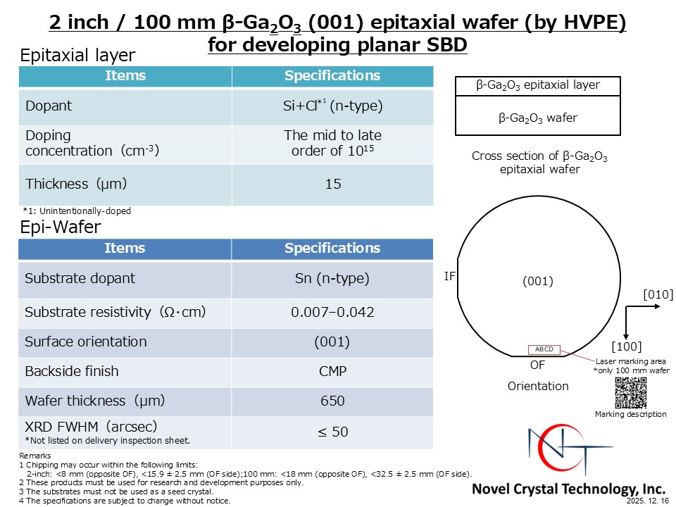
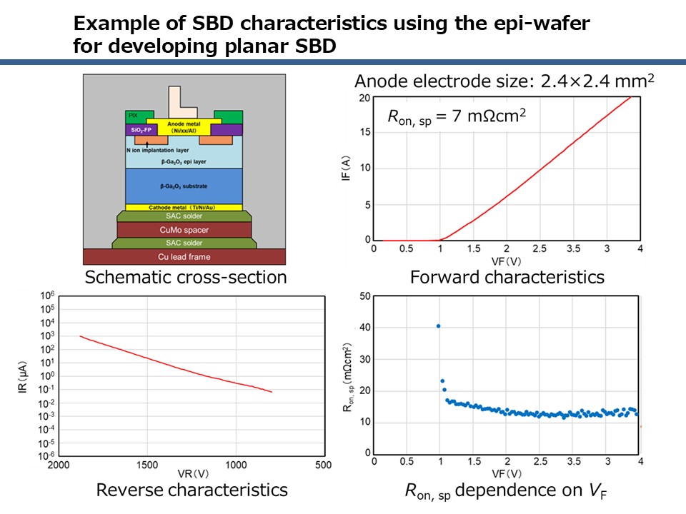
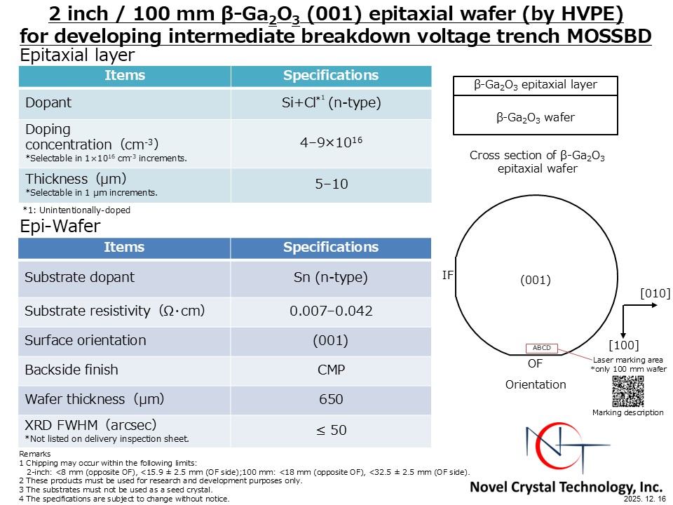
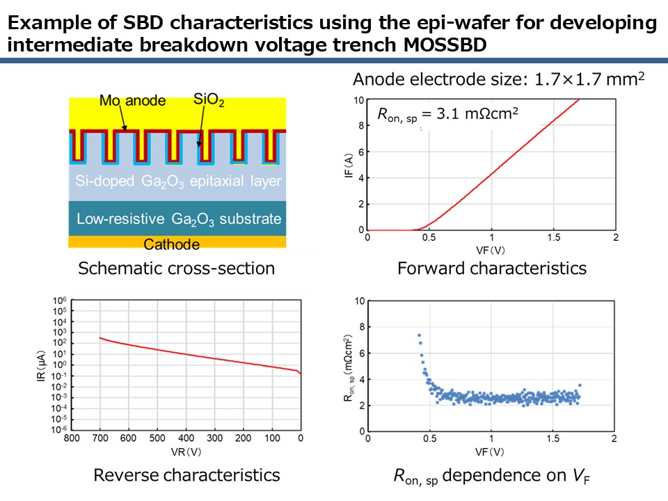
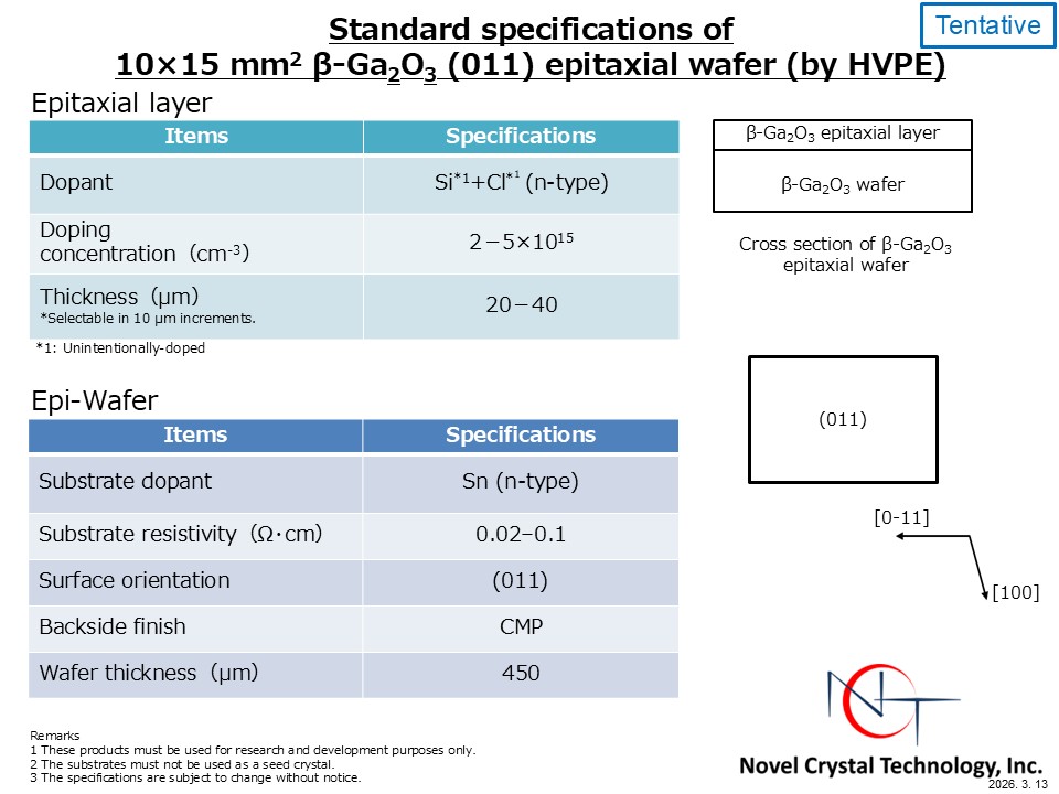
NCT’s β-Ga2O3 HVPE (Halide Vapor Phase Epitaxy) epitaxial wafers are designed for research and development of next-generation power devices, including Schottky barrier diodes (SBD) and transistors.
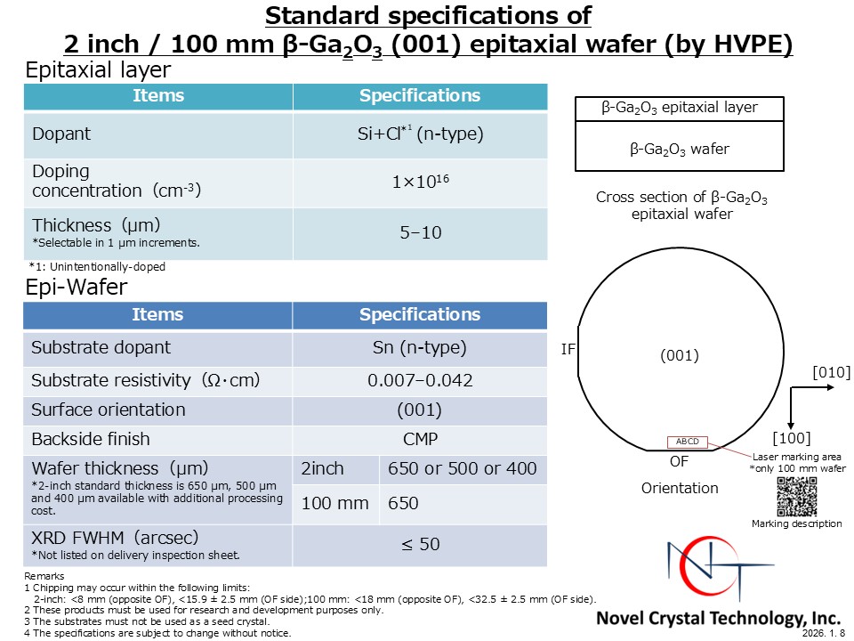
Available orientations include (001) in 2-inch and 100 mm, and (011) in 10×15 mm2 and 2-inch. Si-doping is available for 2-inch and 100 mm (001) epitaxial wafers. Epitaxial doping concentration and thickness can be customized within our technical capabilities.
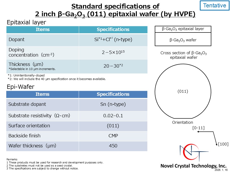
The specification for a 40 µm epitaxial layer thickness for the 2-inch (011) epitaxial wafer will be added to the datasheet once its commercial availability is confirmed.
2-inch / 100 mm β-Ga2O3 (001) epi-wafer (by HVPE)
10×15 mm2 β-Ga2O3 (011) epi-wafer (by HVPE) *tentative
2-inch β-Ga2O3 (011) epi-wafer (by HVPE) *tentative