価格や納期についてはお電話またはお問合せフォームよりご質問ください。
Standard specifications of gallium oxide epitaxial wafer
Epitaxial layer (Growth method: MBE)
| Property | Specification | |
|---|---|---|
| Dopant | Si(n-type) | Undoped(semi-insulating) |
| Doping concentration | Specify a value in the range between 5x10¹⁶ and 2x1018 cm-3 | - |
| Thickness | Specify a value in the range between 0.1 and 0.5 μm | |
Wafer
| Property | Specification | |
|---|---|---|
| Dopant | Sn(n-type) | Fe(semi-insulating) |
| Doping concentration | 1~9x1018 cm-3 | - |
| Resistivity | - | ≧1010 Ωcm |
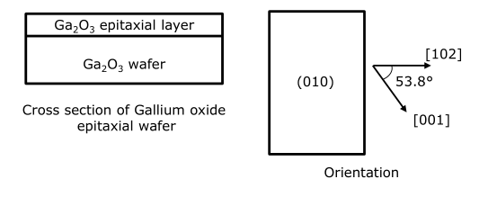
| Orientation | (010) | |
| Size | 10x15 mm2 | |
| Thickness | 0.5 mm | |
| XRD FWHM | ≦150 arcsec | |
| Off set angle | 0°±1° | |
Remarks
1 These products must be used for research and development purposes only.
2 The substrates must not be used as a seed crystal.
3 The specifications are subject to change without notice.