
The world’s first ampere-class 1200-V breakdown-voltage gallium oxide Schottky barrier diode
– A leap toward higher output and lower loss quick chargers, next-generation EVs, and flying cars –
Novel Crystal Technology, Inc., which is working on the commercial development of β-Ga2O3 Schottky barrier diodes as part of NEDO’s “Strategic Energy Conservation Technology Innovation Program”, is pleased to announce its achievement of an ampere-class 1200-V breakdown-voltage Schottky barrier diode (SBD). This achievement will be epoch-making. It will greatly advance the commercialization of gallium oxide SBDs with high breakdown voltages and will lead to lower priced and higher performance power electronics.

Figure 1. Photograph of ampere-class 1200-V withstand-voltage gallium oxide
Schottky barrier diode manufactured on a 2-inch wafer.
In addition, by enabling more efficient and miniaturized power electronics devices such as power converters for photovoltaic power generation, general-purpose inverters for industrial use, and power supplies, this SBD is expected to contribute to the efficient use of electric energy such as through electrification of automobiles and flying cars. The details of this achievement were published in the online version of Applied Physics Express published by the Japan Society of Applied Physics on December 15, 2021.
1. Overview
Gallium oxide (β-Ga2O3) *1 has superior material properties and has a less costly crystal growth method than that of silicon carbide (SiC) *2 or gallium nitride (GaN) *3, which are competing high-performance materials to replace silicon. Low-loss, low-cost power devices*4 can be made from β-Ga2O3, and it is expected that they can be used in home appliances, electric vehicles, railway vehicles, industrial equipment, solar power generators, and wind power generators. Research and development on β-Ga2O3 is accelerating at domestic and overseas companies and research institutes with the goal of using this material to miniaturize and improve the efficiency of electrical equipment.
Novel Crystal Technology, Inc. embarked on its plan to commercialize β-Ga2O3 devices in 2017, and it has been working on demonstrating β-Ga2O3 Schottky barrier diodes (SBDs)*5 as part of the Strategic Energy Conservation Technology Innovation Program of the New Energy and Industrial Technology Development Organization (NEDO). Using our research prototype line and a foundry, we have developed a mass-production process for trench-type*6 β-Ga2O3 SBDs on 2-inch wafers and have developed the first ampere-class 1200-V breakdown-voltage β-Ga2O3. It is expected that high-voltage β-Ga2O3 SBDs arising from this development will have applications such as next-generation quick chargers, for which the need for higher voltage and higher power will increase in the future.
There is a substantial history behind this achievement. Tamura Corporation, the parent company of Novel Crystal Technology, Inc., succeeded in developing the world’s first β-Ga2O3 epitaxial wafers for power devices in 2015 through its participation in a NEDO-funded project, “Strategic Energy Conservation Technology Innovation Program / Research and development of ultra-high voltage gallium oxide power device,” from 2011 to 2013. Since 2018, we have been developing practical β-Ga2O3 SBDs for power devices in the NEDO-funded project, “Strategic Energy Conservation Technology Innovation Program / Research and development of ampere-grade gallium oxide power device.” The success reported here is based on the results of another NEDO-funded project, “Strategic Energy Conservation Technology Innovation Program / Commercial development of β-Ga2O3 SBD” that Novel Crystal Technology, Inc. has been participating in since 2020. The details of this achievement were published in the online version of “Applied Physics Express” published by the Japan Society of Applied Physics on December 15, 2021.
2. Our Achievements
Until now, the planar type*7 structure, which is relatively easy to process, has been used for high-current β-Ga2O3 SBDs. However, since the planar type has a large leakage current*8, it is difficult to manufacture a planar Ga2O3 SBD with a breakdown voltage*9 of 1200 V. In 2017, Novel Crystal Technology, Inc. succeeded in demonstrating a trench-type Ga2O3 SBD that reduces reverse leakage current to 1/1000, and since then, it has been improving the device’s breakdown voltage and increasing the current.
Figure 2 is an optical image and a schematic cross-section of the developed β-Ga2O3 field-plated trench MOSSBD. The device has a forward current*10 IF of 2 A (VF = 2.0 V) (Fig. 3a), breakdown voltage of 1200 V, and low leakage current <10-9 A (Fig. 3b). At present, we are able to mass produce SBDs on 2-inch wafers by using a research prototype line and a foundry.
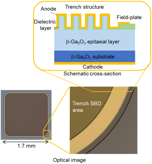
Figure 2. Optical image and schematic cross-section of the developed
β-Ga2O3 field-plated trench MOSSBD
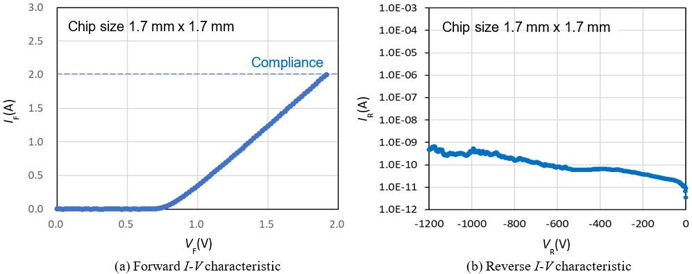 Figure 3. Current-voltage characteristics of the developed β-Ga2O3 field-plated trench MOSSBD
3. Future plans
Through its participation in NEDO projects, Novel Crystal Technology, Inc. will establish the manufacturing process and ensure the reliability of these new 1200-V breakdown-voltage β-Ga2O3 SBDs, aiming for commercialization in 2023. We will also build a 100-mm mass-production foundry line for high-quality β-Ga2O3 100-mm epitaxial wafers, which started to go on sale in June 2021.
The market for medium- and high-voltage high-speed diodes, which is expected to expand to 120 billion yen in 2022 and 150 billion yen by 2030*11 would especially benefit from this development. Novel Crystal Technology, Inc. will enter this market with its β-Ga2O3 SBDs and contribute to the energy-saving society.
[Notes]
1 Gallium oxide (β-Ga2O3)
A compound of gallium and oxygen, it is one of the wide-gap semiconductors.
2 Silicon carbide (SiC)
A compound of silicon and oxygen, it is one of the wide-gap semiconductors.
3 Gallium nitride (GaN)
A compound of gallium and nitrogen, it is one of the wide-gap semiconductors.
4 Power device
A semiconductor element capable of withstanding high voltage and high current, it is used in power conversion equipment such as inverters.
5 Schottky barrier diode
A diode that utilizes rectification, which is called a Schottky junction, in which current flows in only one direction when a semiconductor and metal are bonded. Schottky junction diodes have lower switching losses than those of PN junction diodes.
6 Trench type
A structure in which a groove is formed in Ga2O3 just below the anode electrode. When a reverse voltage is applied, the electric field strength near the anode electrode decreases, which has the effect of significantly reducing the leakage current.
7 Planer type
Ga2O3 is flat just below the anode electrode. When a reverse voltage is applied, the electric field strength near the anode electrode is large and the leakage current increases.
8 Leakage current
The current that flows from the cathode to the anode.
9 Pressure resistance
The voltage limit when a positive voltage is applied to the cathode with respect to the anode.
10 Forward current
The current that flows from the anode to the cathode.
11 Quoted from Fuji Keizai
Quoted from Fuji Keizai “2021 Current Status and Future Prospects of the Next Generation Power Devices & Power Electronics Related Equipment Market”
[Contact]
(Contact for inquiries regarding the contents of this news release)
Novel Crystal Technology, Sales Division:
Contact Person: Masui, TEL:+81-3-6222-9336
NEDO Energy Conservation Technology Department, Development group I:
Contact Person: Kitai, TEL:+81-44-520-5281
Novel Crystal Technology is a carve-out venture of Tamura Corporation, who performs the development, manufacture, and sales of β-Ga2O3 substrates and epitaxial wafers. It is a technology transfer venture of the National Institute of Information and Communications Technology (NICT).